MATERIALS SCIENCE OF SEMICONDUCTOR SILICON
Ten years activity of the International Training Institute for Materials Science (ITIMS) have created marvelous opportunities for ten years of Intensive and Thorough Investigations of Metals in Semiconductors (ITIMS). In a fruitful collaboration between the ITIMS Institute and the Van der Waals-Zeeman Institute of the University of Amsterdam (UvA) a research program on materials science aspects of metallic impurities in semiconductor silicon has been implemented. The element silicon in its covalent crystalline form is by far the most important semiconductor when the field of applications is considered. The electrical and optical functions as required in modern solid state electronic equipment, such as computers, telecommunication units and solar cells, are provided by silicon devices. Millions of diodes and transistors, integrated on large scale on semiconductor wafers, form the heart of processors and memories. Semiconductors owe their importance in technology by the feature that the electrical conductivity can be controlled in the growth process of the material. A choice can be made between electron or hole conductivity by either donor or acceptor doping. The level of steady state conductivity is determined by the amount of doping with impurities with shallow levels, i.e., electronic levels close to either the conduction or valence bands. Trapping and recombination of carriers, governing the transient behavior of devices, is controlled by centers with the electronic levels more deep in the band gap. Modern crystal growth and doping techniques, such as Czochralski pulling, molecular beam epitaxy and ion implantation, allow a great variety of devices to be constructed enabling the desired functions to be implemented. Naturally, for this to be technically feasible, a thorough understanding of impurity and crystal structure defect properties is required. As shown in Table 1, a key feature in modern semiconductor science and technology is the steady trend of reduction in size of structures. Moore’s Law expressing an increase by factor four of integrated elements per every three years, with accompanying increasing complexity in devices and circuits, was followed for several decades and is expected to hold for still some future time. Understanding of impurities and defects in silicon under the new conditions offered by structures with dimensions of only nanometers will be a crucial challenge. Experimental studies as carried out in the ITIMS-UvA program, using the techniques of deep-level transient spectroscopy (DLTS), electron paramagnetic resonance (EPR) and photoluminescence (PL), are intended to provide such knowledge. In past years the focus has been on transition metal impurities with their valence electrons in partially filled d or f shells, as they have a strong local effect on the bonding structure in the crystal, with consequences for electronic and optical properties. Among the elements studied are copper (3d), silver (4d), palladium (4d), platinum (5d), gold (5d) and erbium (4f).
Table 1. Semiconductor Industry Association Roadmap on VLSI technology
Year 1995 1998 2001 2004 2007 2010
Device parameter
Design rule (nm) 350 250 180 130 100 70
DRAM memory size (Gb) 0.064 0.256 1 4 16 64
DRAM chip size (mm2) 190 280 420 640 960 1400
Microprocessor chip size (mm2) 250 300 360 430 520 620
Wafer requirement
Wafer diameter (mm) 200 200 300 300 400 400
Particles per wafer 50 40 50 40 35 20
Particle size (nm) 120 80 60 40 30 20
Deep-level defects in silicon studied by DLTS and EPR spectroscopy
Doctor thesis Pham Nguyen Hai
University of Amsterdam, 20 May 1997
Deep level centers are responsible for lifetimes of carriers and have a dominating effect on the frequency dependence of device performance. Deep-level transient spectroscopy (DLTS) is a sensitive method for detection and characterization of electronic defects in semiconductors. The DLTS method is performed on semiconductor devices which possess a voltage-adjustable space-charge layer. Defects are observed by the electrical response of a device, such as current or capacitance, to the thermal emission of trapped charge. In principle, the technique can distinguish between majority and minority carrier traps and can provide a parameterization of a defect in terms of thermal activation energies, capture cross-sections for carrier-defect interactions, and the concentration and spatial distribution of the deep energy states. For our studies platinum was diffused into p+-n-n+ silicon diodes. Using DLTS, four levels associated with platinum in these silicon devices were detected, respectively at EC – 0.24 eV, EC – 0.57 eV, EV + 0.27 eV and EV + 0.35 eV. Concentrations and capture cross-sections for the majority carriers were determined. The midgap level can be considered to be responsible for the efficient killing of the lifetime in the device.
Most detailed information on microscopic structure of centers is obtained from electron paramagnetic resonance (EPR). Hyperfine interactions with isotopes with non-zero nuclear spin allow unambiguous identification of chemical elements forming part of centers. Angular dependence patterns with respect to crystallographic axes reveal, again in a unique way, the symmetry of a center. Applying EPR, in silver-doped silicon two new centers were discovered [1]. The first, and most basic one, with associated EPR spectrum Si-NL56, arises from an isolated substitutional silver atom, in an orthorhombic-I symmetry distorted configuration. A second center, with spectrum Si-NL-57, is identified as a silver–aluminium impurity pair with trigonal symmetry. The highly mobile copper impurity is observed in a more complexed form [2]. A spectrum, Si-NL58, with the rare tetragonal symmetry, is ascribed to a copper-copper pair. Spectrum Si-NL59 corresponds to a not yet fully identified complex center with one copper atom.
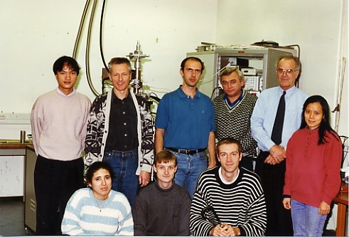
Figure 1. ITIMS scientists dr Pham Nguyen Hai and Du Thi Xuan Thao at the inauguration of the new 140 GHz magnetic resonance spectrometer at the University of Amsterdam. In front, from left to right: dr Ingrid Zevenbergen, dr Frank Berg Rasmussen, Ruud Dirksen. Standing in second row, from left to right: dr Pham Nguyen Hai, dr Tom Gregorkiewicz, dr Ioannis Tsimperidis, ir Vladimir Krymov, prof. dr Rob Ammerlaan, dr Du Thi Xuan Thao.
Photoluminescence spectroscopy on erbium-doped and porous silicon
Doctor thesis Du Thi Xuan Thao
University of Amsterdam, 11 February 2000
Light emission is a most important feature of an electronic material when it comes to application. Unfortunately, related to the character of its electronic band structure, pure bulk silicon has some fundamental handicaps. The band gap value of 1.2 eV restricts the wavelength of band-to-band transitions to the infrared region, larger than 1.0 μm. Due to the indirect character of the conduction to valence band gap, the transition probabilities are low and light intensities small.
A way to overcome the problem of low efficiency is the use of radiant transitions in dopant impurities. Among these options, the rare-earth impurities offer a wide scale of energies. Especially erbium doping is an important area of investigation and application as the prominent transition has the energy 800 meV, which coincides with the region of best transparency of silica optical fibers used in long distance signal transport. Much could be learned about the underlying physical processes from the excitation power and temperature dependence in samples prepared under different conditions. Our experimental observations were analyzed on the basis of a physical model which includes the formation of free excitons, the binding of excitons to erbium ions, the excitation of 4f inner-shell electrons of erbium ions and their subsequent decay by light emission [3]. It was found necessary to consider non-radiative Auger processes in which energy is dissipated to conduction band electrons.
Reducing the dimensions of silicon crystals to become quantum wires or quantum dots leads to an enlarged and direct band gap, with transition energies corresponding to visible light. Our research was based on so-called free-standing yellow fibers prepared by an electro-chemical process. Porous silicon gives photoluminescence in the visible range with intense emission efficiency at room temperature. Very recent results at ITIMS underline the promises of nanostructures by the observation of strong visible light from silicon nanocrystals prepared by sputtering and embedded in a silicon-dioxide matrix. These results offer fascinating prospects for continued research and application.
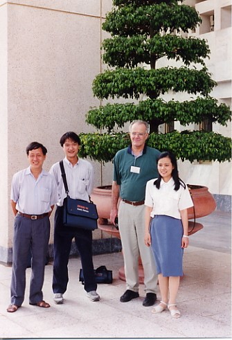
Figure 2. At the 2nd International Workshop on Materials Science in Hanoi, 1995. From left to right: prof. dr Dam Trung Don, dr Pham Nguyen Hai, prof. dr C. A. J. Ammerlaan and dr Du Thi Xuan Thao.
Hydrogen interaction with impurities in silicon
Doctor thesis Pham Thanh Huy
University of Amsterdam, 26 November 2001
After the first observations of hydrogen passivation of defect levels in silicon, reported in the nineteen-eighties, hydrogen as a multipurpose impurity in silicon, with either beneficial or detrimental effects, has attracted enormous research interest. Due to its small size and the open lattice of the diamond structure the hydrogen atom or ion easily penetrates the bulk of the material, a process which can occur unintentionally during process steps in device fabrication. Due to its half-filled 1s electronic shell the hydrogen atom has a high reactivity and as a result hydrogen is involved in a rich variety of defect interactions, forming new centers with new electronic or optical properties. Substantial amounts of hydrogen in the active regions of devices will have a dramatic effect on specifications. As an example, passivation of dangling bonds is used to great advantage for improving carrier lifetimes in less-expensive polycrystalline or amorphous solar cell materials.
A typical illustration of impurity passivation is the, early discovered, bonding of hydrogen to the shallow acceptors, boron, aluminum, gallium and indium, in silicon. The acceptor-hydrogen complexes have no levels in the band gap, with the consequence that all acceptor activity has been removed. Also, hydrogen passivation of shallow donors takes place, though it is not as stable. An interesting case appears with the interaction of hydrogen and double donors and acceptors. Here one expects a possibility of binding one or two hydrogen atoms, possibly correlated with partial and full passivation of the dopant atoms. In our research we investigated the double donors sulfur and selenium by magnetic resonance [4]. Indeed, new chalcogen-hydrogen complexes were detected, all with a trigonal arrangement of atoms along a crystallographic <111> axis. The EPR and ENDOR spectra Si-NL60 and Si-NL61 allowed a full atomic and electronic characterization of the new selenium-hydrogen centers.
Passivation of centers with deep levels is another effect of high technological relevance, as such centers control carrier lifetimes. At the same time hydrogen bonding in deep localized states provides challenging aspects of fundamental physics. In our investigations of 4d transition metals silver and palladium, and of 5d metals platinum and gold, a multitude of new centers from their corresponding magnetic resonance spectra was discovered. Center Si-NL62 is a serious new candidate for identification with the single isolated substitutional gold atom [5]. For platinum the binding of three hydrogen atoms was established for center Si-NL65 Center Si-NL50, the identity of which has raised already strong debate in the literature, has been observed again in silver-doped silicon. Studies in these systems deserve to be continued.
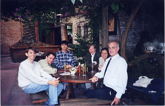
Figure 3. In Berkeley, California, USA, at the 20th International Conference on Defects in Semiconductors. From left to right: dr Peter Stallinga, Bartek Pawlak, dr Pham Thanh Huy, dr Tom Gregorkiewicz, dr Du Thi Xuan Thao, prof. dr Rob Ammerlaan.
References
[1] Electron-paramagnetic resonance study of silver-induced defects in silicon, P. N. Hai, T. Gregorkiewicz, C. A. J. Ammerlaan and D. T. Don, Phys. Rev. B 56 (1997) 4614–4619.
[2] Copper-related defects in silicon: electron-paramagnetic-resonance identification, P. N. Hai, T. Gregorkiewicz, C. A. J. Ammerlaan and D. T. Don, Phys. Rev. B 56 (1997) 4620–4625.
[3] Photoluminescence of erbium-doped silicon: excitation power and temperature dependence, D. T. X. Tao, C. A. J. Ammerlaan and T. Gregorkiewicz, J. Appl. Phys. 88 (2000) 1443–1455.
[4] Hydrogen passivation of the selenium double donor in silicon – a study by magnetic resonance, P. T. Huy, C. A. J. Ammerlaan, T. Gregorkiewicz and D. T. Don, Phys. Rev. B 61 (2000) 7448–7458.
[5] Magnetic-resonance investigation of gold-doped and gold-hydrogen-doped silicon, P. T. Huy and C. A. J. Ammerlaan, Phys. Rev. B 66 (2002) 165219-1/12.
TG: A. J. Ammerlaan, P. N. Hai, D. T. X. Thao and P. T. Huy
